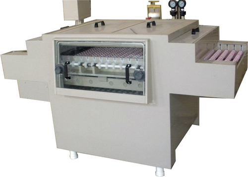
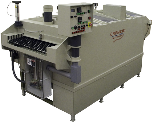
Etching inner layer in PCB production
We remove the unwanted copper using a powerful alkaline solution to dissolve (or etch away) the exposed copper from the inner layer. The process is carefully controlled to ensure that the finished conductor widths are exactly as designed. But designers should be aware that thicker copper foils need wider spaces between the tracks. The operator checks carefully that all the unwanted copper has been etched away.
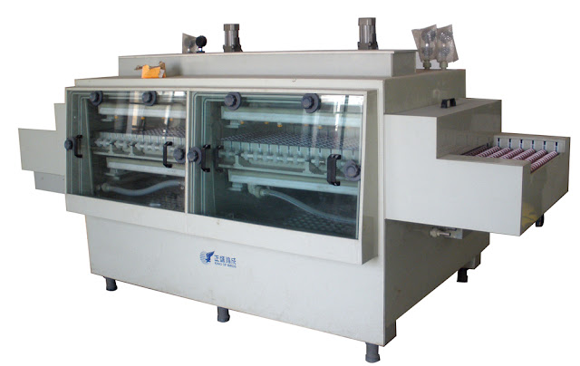
Next we strip off the blue photoresist which protected the copper image. So now we have the exact pattern required. The operator checks that all the photo-resist has been removed. You can see that Eurocircuits put several different designs on one production panel. That way we can make small numbers of PCBs cost-effectively.
Next we strip off the blue photoresist which protected the copper image. So now we have the exact pattern required. The operator checks that all the photo-resist has been removed. You can see that Eurocircuits put several different designs on one production panel. That way we can make small numbers of PCBs cost-effectively.
best ayurvedic treatment centre in delhi
ReplyDeleteThanks for your valuable comment,here is an amazing best diabetes doctor in delhi ncr
ReplyDelete